

| Quantum Well Infrared Photodetectors (QWIP)
Quantum Well Infrared Photodetector DevelopmentThe advanced multispectral quantum well infrared detectors (QWIPs) developed at CQD can revolutionize infrared imaging. 
The technology developed at CQD can provide low-cost medical thermal imaging. We have characterized and optimized the performance of QWIPs fabricated from quantum wells or barriers of AlGaInAs or GaInAsP material and made comparisons with that achieved with the more mature GaAs/AlGaAs device design. In order to demonstrate new functionality, such as the possibility of multispectral detection, we have investigated several different designs based on heterostructures of InGaAs/InP, InGaAs/InAlAs, and AlGaInAs/InP.
InP-related quantum well infrared photodetectors cover the range 3>λ>20 μm. InGaAs/InP QWIPsThree identical InGaAs/InP QWIP series (λ=9 μm) were grown by LP-MOCVD with three different quantum well doping densities. The optimal detectivity came from the series with ND = 5.0x1017 cm-3. This series had a responsivity of 33.2 A/W and operated with a detectivity of 3.5x1010 cm·Hz½/W at a bias of 0.75 V. This responsivity is to our knowledge the highest value reported for any QWIP in the λ=8~9 μm range without any additional light coupling enhancement feature. To improve the light coupling efficiency for such QWIPs, we utilized a corrugated structure. The corrugated pattern was made by electron-beam lithography and ECR-RIE dry-etching. Very high peak responsivity of 218 A/W wasachieved for a ~8 μm InGaAs/InP QWIP with a corrugation period of 10 μm. InGaAs/InAlAs QWIPsWe presented optimization of the device design for InGaAs/InAlAs QWIPs for mid-wavelength infrared detection. These MWIR detectors demonstrate high detectivity, and have a constant responsivity up to T = 200 K. The fact that they are lattice-matched to InP has allowed us to demonstrate the first InP-based multispectral detector for 3~5 and 8~9 μm detection. We additionally presented QWIPs fabricated from the AlGaInAs/InP material system that is sensitive to the spectral region between λ=8~20 μm when the Al mole fraction is varied from 0 to15 %. AlGaInAs/InP QWIPsWe have demonstrated the first preliminary QWIP detectors using the quaternary InGaAsP/InP materials system growth by MOCVD. By increasing the bandgap from ternary InGaAs to quaternary InGaAsP we have shifted the responsivity out to longer wavelengths resulting in cutoff wavelengths of 10.7 and 14.2 μm for Asmole fractions of 0.80 and 0.57, respectively. For the device with a 10.7 μm cutoff wavelength, we have observed responsivity as large as 1.09 A/W at a bias of 2 V. The conduction band offset for these samples is ~ 0.32, smaller than the typically reported value of 0.40. InGaAs/InP QWIPs on SiLastly, the direct growth of InGaAs/InP superlattices on Si substrates was investigated to take advantage. Through optimization, QWIP-on-Si photodetectors were realized with a record high detectivity of 2.3x10⁹ cmHz½/W. These exhibited much better detector performance than GaAs/AlGaAs QWIP-on-Si. Multi-Spectral QWIPsThe advanced multispectral quantum well infrared detectors QWIPs) developed at CQD have been successfully used to realize multi-spectral photodetectors. By combining MWIR and LWIR QWIP structures, researchers at CQD demonstrated the first multi-spectral QWIP detectors on InP substrate. This QWIP structure was composed of MWIR 20 periods InGaAs/InAlAs multi-quantum wells (MQW) and 20 periods LWIR InGaAs/InP multi-quantum wells on semiinsulating InP substrate. 
Spectral response for a two-color QWIP at T=77 K for different biases. For a bias <7 V, only one peak at 8.5 μm was observed. for higher biases, a peak at 4 μm was observed. At low biases, the electric field is applied mostly across the lower resistance LWIR InGaAs/InP MQW. At higher biases, the electric field is applied across both MQWs but no photoresponse was observed for InGaAs/InP MQW then since most carriers in the ground states of this MQW tunnel out before absorption occurs. 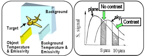 One of the application of such detector is target recognition. Each object has it's unique infrared radiation pattern or "signature". This pattern consists of different intensities at different wavelength and hence multi-spectral infrared imaging is the only method to distinguish the signature of a certain object from the background. This is an important issue for many medical and military applications where one wants to recognize a target from the background. One example of this situation is illustrated on the right when the infrared radiation of the airplane is identical to the sky at 8 μm wavelength, while there is a high contrast at 10 μm. QWIP Focal Plane Arrays for Imaging
QWIP focal plane array being tested. The Center for Quantum Devices has all of the necessary facilities for the fabrication and testing of focal plane arrays (FPAs), including wafer dicing, indium plating/evaporation, flip chip bonding, array hybridization, and mechanical lapping and polishing. The FPA testing equipment includes a LN2 dewar, a camera head, and digital electronics. The testing system from SE-IR Corp. can test up to 800x600 single color arrays, 512x512 two color arrays, and 320x256 four color arrays. Researchers at CQD have developed FPAs for LWIR InAs/InP QWIPs and MWIR InGaAs/InAlAs QWIPs. Both 256x256 (Litton ROIC) and 320x256 (Indigo ISC9705 ROIC) format FPAs have been developed with a detector size of 25 μm and a pitch of 30 μm. The FPA substrate was hybridized onto a read-out integrated circuit (ROIC) using indium solder bumps. After thinning the FPA hybrid was bonded to a leadless ceramic chip carrier for testing. 
QWIP focal plane array fabrication steps performed at the Center for Quantum Devices.  
(Left) Indium bump made by indium electroplating method and (right) SEM picture of detector array pixels with an area of 25 x 25 μm2. 
GaInAs/InP QWIP FPA hybrid bonded to a 68 pin LCCC. The first FPA realized at CQD was in the LWIR InGaAs/InP QWIP system. This FPA had mean NEDT of 114 mK at an operating temperature of 70 K and bias of -2.35 V with f/2 optics. A MWIR InGaAs/InAlAs QWIP was also demonstrated with over 99 % working pixels and a mean NEΔT of 54 mK at an operating temperature of 100 K and bias of -2.5 V.  
(Left) Imaging of a person taken by our first LWIR InGaAs/InP QWIP FPA camera.  
(Left) Thermal imaging of a person taken at an FPA operating temperature of 100K. Last Updated 10/08/2008 |
| © 2020 Center for Quantum Devices, Northwestern University Disclaimer |
 Channel
.jpg)