| About the CQD | | News | | Conferences | | Publications | | Books | | Research | | · Quantum Cascade | | · Type-II SLS | | · Quantum Dots | | · III-Nitrides | | · Nanotechnlogy | | · QWIP | | · Uncooled InAsSb | | · InTlAsBiSb | | · Al-Free Lasers | | · Antimony Lasers | | People | | History | | Patents | | Contact |  Channel Channel |
|
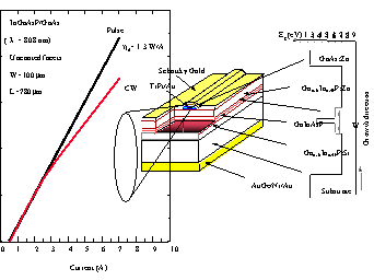
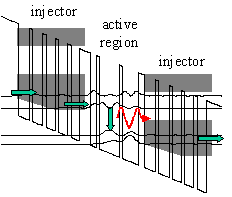 Lasers operating in the mid- and far-infrared (3-16 µm) spectral region are desirable for many applications. Many of these applications are centered around protection of people against various threats. Remote chemical sensing is perhaps the most straightforward and is aimed at detecting toxic chemicals, explosives, and chemical warfare agents at a safe distance. In addition, these lasers are being looked at for safeguarding aircraft against missile attacks as well as for higher reliability free-space communication. Up until recently, the only such laser technologies available were based on bulky gas or solid-state lasers as well as cryogenically cooled semiconductor lasers. One of the most exciting projects at the Center for Quantum Devices is uncooled infrared quantum cascade lasers (QCLs), which, being a semiconductor laser, is inherently compact and will help eliminate the need for bulky and unreliable cryogenic cooling. This translates to a smaller, cheaper, system with a longer lifetime and less maintenance. Besides our current records with respect to operating wavelength range and high peak power, we also have developed the highest power continuous wave QCLs at room temperature. We are currently endeavoring to improve device efficiency, improve spectral and spatial emission characteristics, and to scale the output power to new record levels. ...[read more]
 III-V quantum wells and superlattices based on InAs/GaSb/AlSb, and related compounds have attracted many attentions due to their unique band alignments and physical properties. Recently, novel electronic and optoelectronic heterostructures have been proposed from this material system for hundred gigahertz logic circuits, terahertz transistors, RTDs, infrared lasers, and infrared detectors. At the Center for Quantum Devices, we have developed the theory, modeling, growth, characterization, and device fabrication techniques for this material system which have enabled us to demonstrate some of the best reported results for uncooled and very long wavelength Type-II detectors. ...[read more]
 Wide bandgap III-Nitride materials (AlInGaN) have recently become one of the hottest research topics among the semiconductor community, owing to their excellent potential for use in high-power electronics and UV/ visible optoelectronic devices. The Center for Quantum Devices has played an important role in the develop-ment of III-nitrides, demonstrating world record achievements in both light emitting and light detecting devices (including recent work on photon counting detectors). Much of this research has been funded by the DoD. Some of the most recent and important achievements are highlighted below. ...[read more]
 Semiconductor quantum dots (QDs) are attractive thanks to their exciting electronic properties which significantly impact the performance of high speed electronic and photonic devices, and the development of novel device concepts such as the single electron transistor. Quantum dots, also known as quantum boxes, are nanometer scale islands in which electrons and holes are confined in three-dimensional potential boxes. As a result of strong confinement imposed on all three spatial dimensions, quantum dots are similar to atoms. They are often referred as artificial atoms. One of the approaches investigated at the CQD was to realize QDs through selfassembly during epitaxial growth for the demonstration of photodetectors and lasers. ...[read more]
Si LDMOS has been the dominant transistor technology in cellular base-station power amplifiers for the past 15 years due to its low cost and excellent RF performance. The emerging fourth generation (4G) cellular standard has extended the operating frequencies beyond 2.2 GHz thereby pushing the Si LDMOS technology to its usable limits. The 4G system architecture has shifted to multiple independent transmitters in a single basestation to utilize the multiple antenna technology. The need for high frequency, power, and gain density devices will increase the demand for Si LDMOS RFIC devices that satisfies the requirements for 4G power amplifiers. . ...[read more]
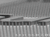 Enhancing the performance and functionality of optoelectronic systems requires smaller device dimensions. However, optical lithography is currently limited to feature sizes around 0.13 µm in commercial IC fabrication. Further reducing the critic al dimension of devices requires the use of high resolution techniques such as electron beam lithography. Features as small as 0.02 µm have been demonstrated using the Leica LION-LV1 electron beam lithography system at the Center for Quantum Devices. ...[read more]
 Realizing an 'artificial eye' in the form of an infrared imaging device is one of the most thrilling projects at the Center for Quantum Devices. The research team is exploring the multi-spectral Quantum Well Infrared Photodetector (QWIP) focal plane array technology for this end. This effort was funded by DoD and is motivated by the potential of this technology in enhancing the performance of medical thermal imaging and unambiguous object identification. ...[read more]
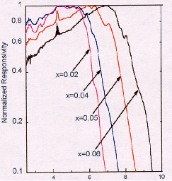
 The Center for Quantum Devices has been involved in the research of InAsSb since its conception. The success-ful development of the III-V material system InAsSb would offer an alternative choice to the industry dominant II-VI material system HgCdTe and thermal detectors such as microbolometers for infrared photodetectors oper-ating between 7 μm and 12 μm for operation at room temperature. Thus, InAsSb, over its composition, overlaps two wavelength ranges where the properties of the atmosphere differ significantly. ...[read more]
 The need for high speed uncooled infrared detectors ignited the research of narrow bandgap compound semicon-ductors. High-speed uncooled infrared (IR) detectors based on this system are highly demanded for many mili-tary and industrial applications such as: target detection systems, proximity fuzes, smart bombs, infrared active countermeasure systems, LIDAR, non-destructive testing and inspection techniques, monitoring of the chemical quality and process control, remote sensing, and free space communication. ...[read more]
 One of the most challenging research projects at the Center for Quantum Devices has been to develop the sci-ence and technology of aluminum-free semiconductor lasers based on the InGaAsP/GaAs material systems. The primary objective of this research work was to out perform commercially available AlGaAs based lasers. The research work was funded by DoD. The technology has been licensed to Industry. Some of the groundbreaking accomplishments are summarized below. ...[read more]
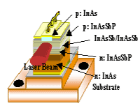 Electrically injected semiconductor mid-infrared (3-5 μm) lasers are strategically important light sources for awide range of military and civilian application systems. For most of these applications, reliable high-power op- eration is critical as it determines sensitivity and spatial range of the final applications. The research conducted at the Center for Quantum Devices is leading the research community in making mid-infrared lasers available for applications. Currently, three types of interband laser structures are considered as promising high power high temperature lasers. ...[read more]
last updated 05/20/2016
|

