| Type-II Superlattice Based Infrared Detectors
Novel Type II superlattice design.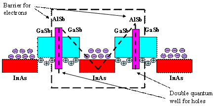
Schematic diagram of the M structure. The inserted AlSb layer forms a barrier for electrons in the conduction band and a double quantum well for holes in the valence band. Type II InAs/GaSb superlattice was first introduced by the Nobel laureate L. Esaki in the 1970s and then proposed for infrared detection applications by Smith and Mailhiot in 1987. Since then, Type II Sb-based superlattice has evolved drastically with many variants for different purposes. We have developed a new superlattice design, called M-structure superlattice, which acquires the beneficial properties of the well established binary – binary antimonide based SL structures used in high performance infrared detectors. First, it conserves the Type – II misalignment of InAs and GaSb, which is capable of eliminating the electron-hole split – off band Auger transition by reducing the resonance between the energy gap and split-off band. Second, the AlSb layer has a large energy bandgap with the conduction band offset higher than that of GaSb and the valence band offset slightly higher than that of InAs. Due to this band offset, AlSb can be utilized as a blocking layer for both electrons in the conduction band and holes in the valence band. As a consequence, the insertion of the AlSb into the GaSb, forming the M – superlattice, will reduce the tunneling probability in long wavelength (LWIR) and very long wavelength (VLWIR) photodiodes because the effective mass of the carriers over the standard binary – binary SL is increased. In comparison with other ternary/quaternary superlattices, such as the WSL or the InAs/GaInSb superlattices, the M structure is easier to realize because it still keeps the simple form of a binary – only structure, which is less sensitive to the growth temperature and the III-V flux ratio. Finally, the growth of the M-structure is as simple as a standard binary – binary InAs/GaSb structure because there is a small mismatch in the lattice constant between AlSb (6.136 Å) and GaSb (6.097 Å) and the common antimony atom allows for a smooth interface between the two layers. The M-structure does not need as much care as the growth of AlSb on InAs in the WSL where the interface of AlSb and InAs have no common atom and AlSb grown on InAs is highly strained. M-structure superlattice has been successfully integrated onto Type II InAs/GaSb superlattice photodiodes and demonstrated orders of magnitude of improvement for the electrical performance of LWIR and VLWIR detectors. Material system with a large variation range of cut-off wavelength.One of the benefits of Type II superlattice is the capability to tune the detection cut-off wavelength in a very wide range. By adjusting the thicknesses of constituent layers, the energy gap of the structure can be precisely controlled with excellent uniformity over a three inch wafer area. We have experimentally demonstrated Type-II InAs/GaSb superlattice photodiodes with cut-off wavelength varying from 3.5mm up to 32mm. The measured results fit nicely with the theoretical prediction using Empirical Tight Binding Model. 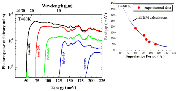
Spectral response of photodiodes with different InAs/GaSb superlattices in their active layer. The thickness of GaSb layer is 40 Å for all of the superlattices, while the thickness of the InAs layer is shown for each device. ETBM calculations agree with experimental data. 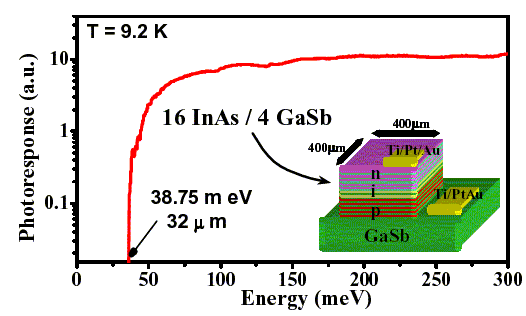
Relative responsivity for Type-II superlattice detectors with cutoff wavelength of 32 μm at T=9.2 K. At the longest cut-off wavelength ( ~32 μm ), the detectors have a peak responsivity of 3 A/W and a detectivity of 4.25 x 1010 cm·Hz½/W at 15 μm under 40 mV reverse bias at 34 K. Ultra Fast Uncooled Infrared DetectorsHigh-speed uncooled infrared (IR) detectors are highly demanded for many military and industrial applications such as: target detection systems, proximity fuzes, LIDARs, non-destructive testing and inspection techniques, monitoring of the chemical quality and process control, remote sensing, and free space communication. Commercially available uncooled IR imaging sensors use ferroelectric or microbolometer detectors which are inherently slow. Although photon detectors have gigahertz bandwidths, their high temperature detectivity is severely degraded due to several physical limitations. The existing infrared photon detectors can be categorized as interband, such as HgCdTe, and intersubband quantum well infrared detectors (QWIP). There are some fundamental limitations, namely fast Auger recombination rate in the interband detectors and high thermal generation rate in the intersubband detectors, which drastically decrease their performance and ability for high temperature operation. At first, we developed the growth of high quality Type-II superlattices. In order to increase the operating temperature of detectors, we designed the superlattices for an effective suppression of Auger recombination, and confirmed it experimentally or the first time. 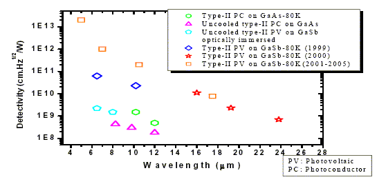
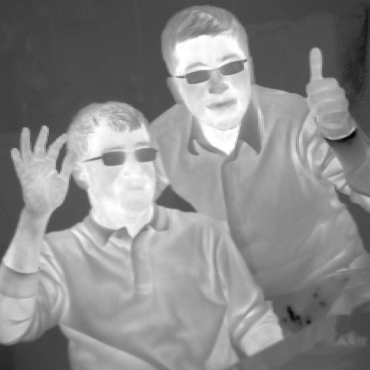
The progress of cooled and un-cooled Type-II detectors at CQD. Using such designs, we demonstrated the first uncooled infrared detectors from Type-II superlattices. The measured detectivity is more than 1x108 cm x Hz½/W at 10.6 μm at room temperature which is higher than the commercially available uncooled photon detectors at similar wavelength. The measured carrier lifetime was about 27 nsec which is an order of magnitude longer than the bulk material due to the suppression of the Auger recombination. To use such devices in focal plane arrays (FPA) for imaging applications, we also developed Type-II photodiodes operating at zero bias. 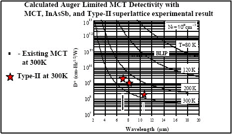
Comparison with the state of the art and with the theoretical Auger limited detectivity. Furthermore, we realized the first uncooled Type-II photodiode at λ=8 μm with a zero bias detectivity of 1 x 108 cm·Hz½/W. Recently we demonstrated uncooled photodiodes with 5 μm cutoff that have a zero bias detectivity above 1 x 109 cm·Hz½/W and a device quantum efficiency exceeding 30 %. These results indicate that Type II superlattice is an excellent candidate for uncooled applications. High performance Superlattice PhotodiodesVery high performance long-wavelength infrared (LWIR or 8~12 μm) and very-long-wavelength infrared (VLWIR, l > 12 μm) detectors and imaging arrays are in high demand for strategic missile defense, pollution monitoring, and space-based astronomy. Material uniformity complexities and strong leakage currents limit the viability of state-of-the-art HgCdTe detectors in this wavelength regime. For this reason, type-II superlattices are being pursued as an alternative third generation focal plane array technology. Intensive research in the LWIR and VLWIR has lifted the performance of Type II superlattice photodiodes to a comparable level to the state-of-the-art HgCdTe technology. High quality material has been obtained, allowing for the very thick device structure without any degradation of the crystallinity. As a results, the absorption length of the photodiodes could be extended, the devices exhibit a quantum efficiency more than 50% for front side, single path configuration, and more than 75% for back side multiple path configurations. 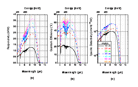
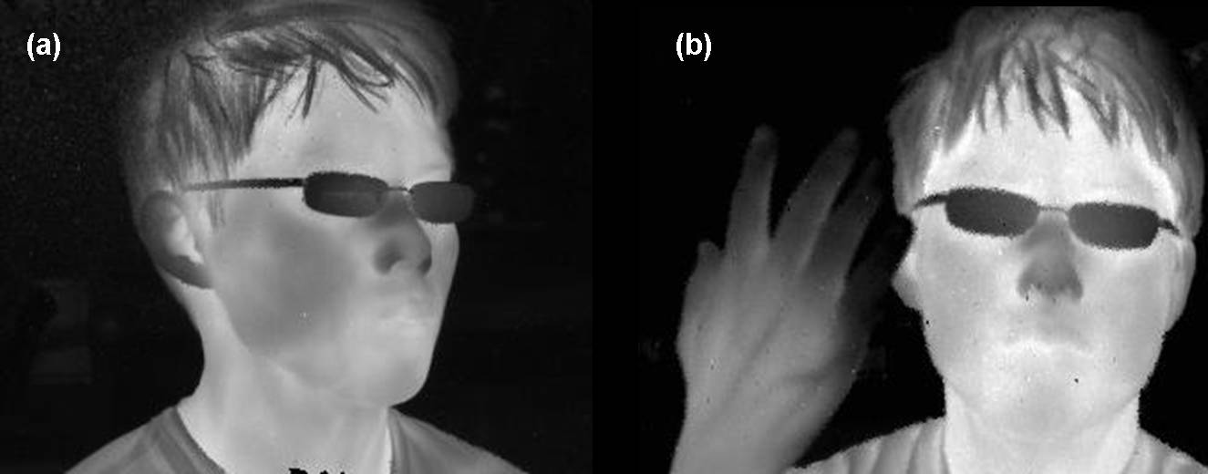
Optical responsivity, Quantum efficiency and specific detectivity as a function of device thicknesses. Thicker device allows for higher optical performance. In attempt to reduce the electrical noise due to the dark current, we developed a new device architecture, where the M-structure superlattice was used as a barrier in between the p and n- regions of the diode. The M-barrier has been shown to efficiently suppress both the tunneling and the diffusion current of the device, leading to an order of magnitude decrease of the dark current. 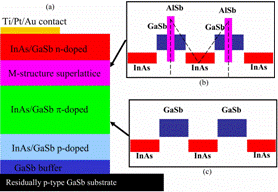
New device architecture with M-structure superlattice for the suppression of dark current. A combination of optimization schemes for the optical and electrical performance enables LWIR devices to be BLIP limited at 110K with a 2p field of view facing a 300K background. The same study can be applied for 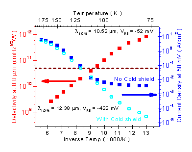
Measurement of BLIP temperature using the delineation of dark current between cold shielded/ no cold shield configurations, and using specific detectivity measurement. Novel Device Architectures
Novel Device Architecture. Recently, a novel device architecture called p-M-p proposed to combine the advantages of photoconductive and photovoltaic detectors. By using the unipolar mode of minority carrier devices, the device was expected to have low generation-recombination current, low tunneling current, and high quantum efficiency at very small applied bias. The proof of concept of the architecture has been demonstrated at the MWIR and VLWIR regime, and exhibit comparable performance to the best MWIR and VLWIR Type-II superlattice photodiodes. The architecture is also beneficial for two color device operating in bias selectable mode World's First High PerformanceType-II Superlattice Focal Plane ArrayBuilding on our extensive experience on this material, we have recently demonstrated the world's first uncooled Type-II mid-wave infrared focal plane array operating with a 5 μm cutoff wavelength. This uncooled camera array operates with 25 % quantum efficiency, a detectivity of 8 x 108 cm·Hz½/W, and a NEΔT of 50 K. 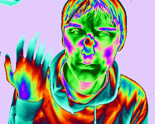 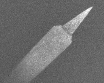
MWIR Type-II InAs/GaSb superlattice FPA imaging obtained at 77 K, left. Uncooled infrared imaging of a hot soldering iron based on MWIR Type-II InAs/GaSb superlattices, right. These superlattice FPAs provide high quality imaging of warm subjects, such as human beings, up to a temperature of about 160 K, significantly higher than the conventional operating temperature of 77 K. It can also provide fast uncooled imaging at room temperature for a hot soldering iron with demonstrated frame rate of 110 Hz and potentially up to 600 Hz. 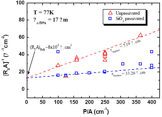
Silicon dioxide surface passivation greatly reduces the surface leakage in VLWIR type-II photodiodes, making focal plane arrays in this wavelength regime a possibility. One obstacle to the technological success of type-II infrared focal plane imaging arrays is solving the ever-present problem of surface passivation. The small dimensions of focal plane array pixels enhance the amount of leakage current caused by surface effects. With a proper electrically passivating layer, surface states can be reduced and leakage current decreased, greatly improving the overall device detectivity and performance. At CQD we have demonstrated successful silicon dioxide passivation in the MWIR, LWIR, and VLWIR on type-II photodiodes. Additionally, we have developed a polyimide-based technique that significantly reduces surface leakage in LWIR devices. 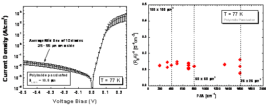
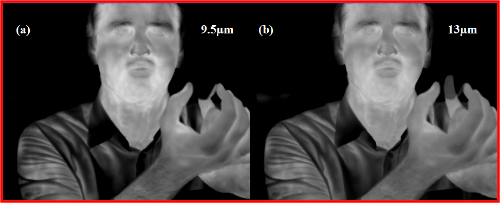
I-V characteristic of small devices passivated with polyimide (left). Variation of the dynamic resistance with the size of the diodes (right). Using our experience for FPA fabrication and our expertise on LWIR type-II InAs/GaSb superlattice single element detectors, we started developing FPAs in the LWIR (8-12μm). As the wavelength increases (the bandgap decreases), the devices become more sensitive to surface effects, making the FPA fabrication process more critical. Thanks to enhancement in our growing, etching, cleaning, hybridation techniques, we managed to fabricate the world's first and best 320x256 FPA based on type-II InAs/GaSb superlattice photodetectors with a cutoff wavelength higher than 8 μm. This FPA with the highest cutoff wavelength demonstrated yet for type-II superlattice is able to perform imaging of human beings from 81 K to 120 K. It can also perform imaging of soldering iron up to 200 K. The array is able to detect temperature differences as small as 20 mK. The quantum efficiency of the array reaches over 80% when an AR coating is deposited. 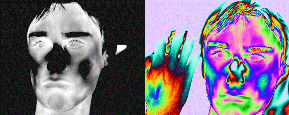 LWIR Type-II InAs/GaSb superlattice FPA imaging obtained at 80K. Based on the development of material and device architecture, an M-barrier heterojunction was designed for high operating temperature (HOT) mid-infrared detection. The device exhibited a 50% cut-off wavelength of 4.9 μm at 150K and a quantum efficiency above 50% in front side illumination. A MWIR camera was fabricated and hybridized to an Indigo ISC9705 Read Out Integrated Circuit and characterized at different temperatures.
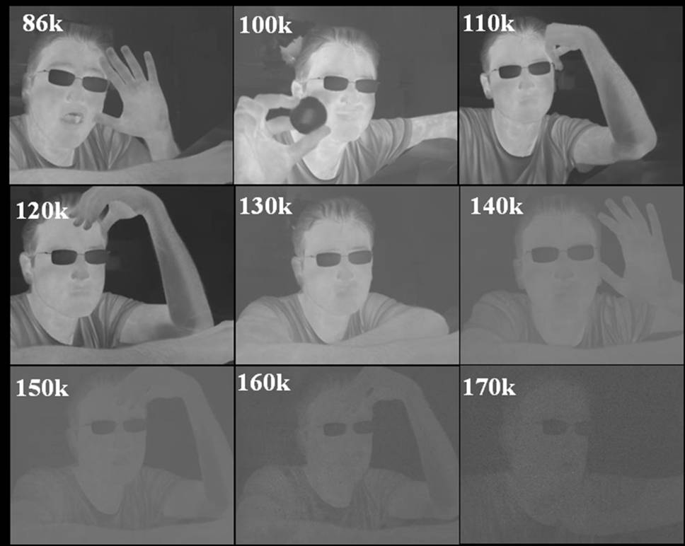
Noise equivalent temperature dependence (NETD), a performance metric dictating the minimum temperature difference that a thermal camera can differentiate, was measured under f/2.3 optics (~16o field of view) and 300K background. Below 120K, the NETD stayed constant at ~10mK for integration time of 10.02 ms, and can be reduced to 8 mK when longer integration time was set. This temperature insensitivity indicates that the camera was limited by either photon noise or system noise rather than shot noise since the later exhibited very strong dependency on temperature. At higher temperature, the dark current increased and became limiting factor to FPA operation. Higher operating temperature led to larger NETD . Human imaging is recognizable when FPA is operated at 170K while uncooled camera can image hot objects such as a soldering iron.
Large Format 1024x1024 LWIR FPAsAdvances in material development have enabled realization of very high quality material with excellent uniformity over large wafer area.
Demonstration of excellent material uniformity over 3" in diameter wafers
Technological challenges of focal plane arrays have been overcome, and resulted in demonstration of the first high performance, large format focal plane array based on Type-II superlattice. The 11 um cut-off FPA showed excellent imaging with a 300 K background at an integration time of 0.13 ms using f/2 optics . A noise equivalent temperature difference (NEDT) of 23.6 mK, a dark current (Jdark) of 3.3 × 10⁻⁴ A/cm2, a differential resistance area product at zero bias (R0A) of 166 Ωcm2 at 81 K and 22.5 mK, 5.1 × 10⁻⁵ A/cm2, 1286 Ωcm2 respectively at 68 K were observed. A quantum efficiency of 78% was obtained.
Demonstration of world first high performance 1kx1k LWIR FPA at 81K
FPAs on GaAs substratesRealization of large format focal plane arrays raises a need for larger size substrates for mass production and cost reduction. While a conventional 2” GaSb substrate can only allocate one 1024x1024 FPA die, a 3” GaSb substrate can allow for a production batch of 4 FPAs. In order to even further reduce the fabrication cost, large size GaAs substrates are desirable since these wafers are commercially available with size upto 6” in diameter and at low cost. However, a challenge for realization of Type-II superlattice FPAs on GaAs substrates is the lattice mismatch of 7% between the superlattice and the substrate, which causes severe degradation of the material quality. Efforts have been paid to overcome this challenge and achieved high quality Type-II superlattice on GaAs substrates. The materials were processed into 320x256 focal plane arrays for both MWIR and LWIR regimes. Excellent imaging quality was demonstrated with cameras cooled to 67K.
Demonstration of world first high performance FPAs based on T2SL grown on GaAs substrates: a) MWIR b) LWIR.
Dual band LWIR FPAsHigh performance single color FPA have been already demonstrated for the LWIR regime. However, despite the high performance, single band FPAs are sometimes unable to discriminate a target from its background when they present similar infrared radiation at a given wavelength. This may occur even if the temperature of the object is very different from the background temperature. In such a case, two color FPAs offer an additional wavelength that allows easy identification of the target.
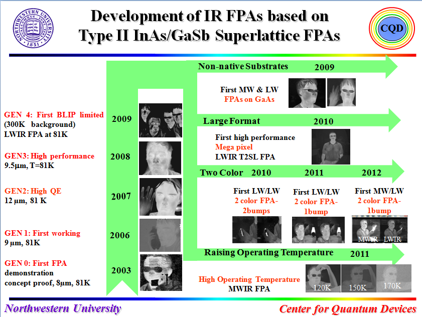
Summary of development for third generation FPAs
|
| © 2020 Center for Quantum Devices, Northwestern University Disclaimer |
 Channel
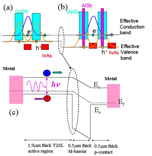
.jpg)